
A center of excellence blending academic research and industrial innovation, dedicated to advanced electronic design, sensing, and long-term space missions.
With the inauguration of the Nanolabss joint lab, a new hub of excellence in mixed-signal electronic design and advanced microelectronics takes shape. Conceived as a space for research, experimentation, and strategic vision, Nanolabss is more than just a technological laboratory; it is a true think tank where academia and industry collaborate to envision and develop the technologies that will drive next-generation sensing and future scientific space missions, even decades from now.
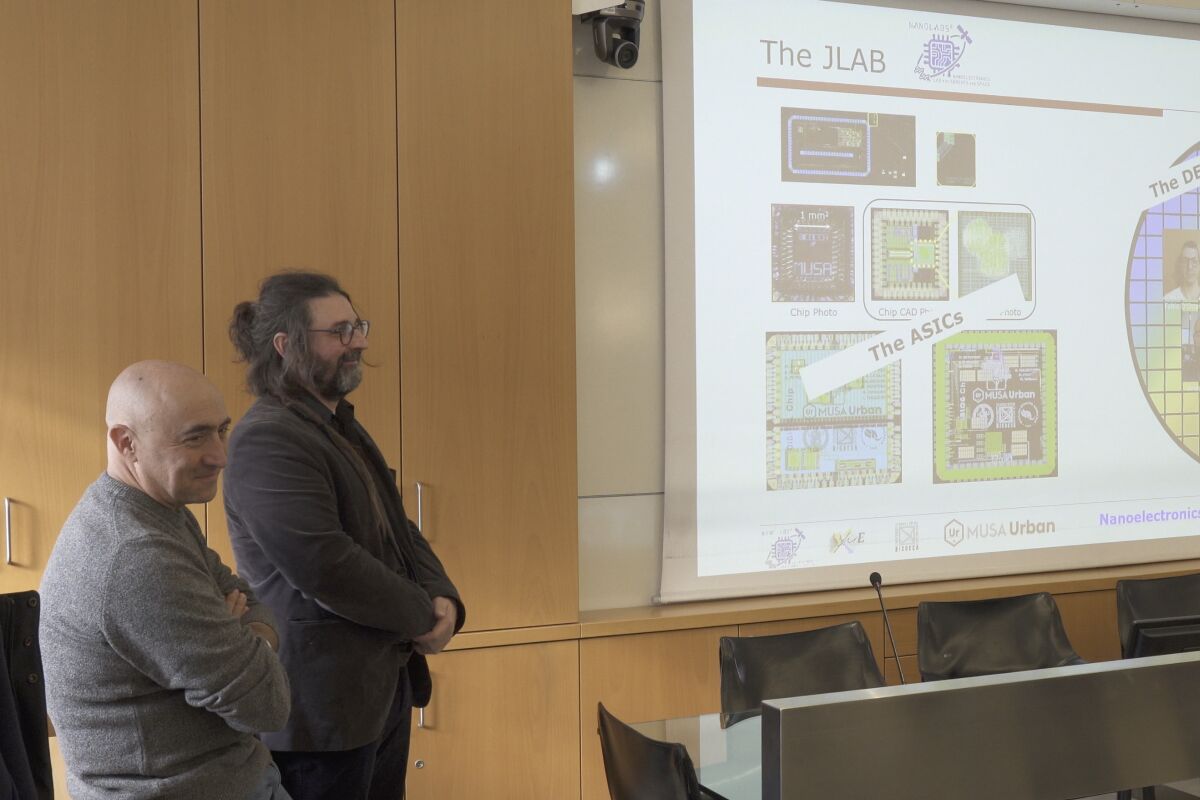
At the heart of Nanolabss is R&D in the field of electronic design, with a specific focus on the digital design of open-source microprocessor architectures and ultra-high sensitivity analog front-ends used in frontier applications such as nanogravimetry. Alongside this, the laboratory is committed to developing Application-Specific Integrated Circuits (ASICs) using state-of-the-art CMOS technologies, ranging from 7nm and 16nm FinFET nodes to 28nm and 65nm planar processes. This scope also includes a strong specialization in radiation-hardening methodologies—a crucial expertise for the aerospace sector and any context where extreme reliability is an absolute requirement.
The joint lab’s activities are led by a team consisting of Marcello De Matteis (Head of Micro and Nanotechnology at the JLAB), Mario Zannoni (Laboratory Coordinator), and Mattia Tambaro (Researcher). Together, they pursue a multidisciplinary vision that extends beyond microelectronics in the strict sense.
Indeed, Nanolabss serves as an exploration ground for emerging technologies, such as next-generation thermal sensors, microfluidic concepts for energy harvesting in space, and the integration of satellite remote sensing data with ground measurements. These diverse activities share a common mission: to anticipate innovation, explore ideas from their most embryonic stages, and align long-term scientific vision with industrial strategies.
The joint lab is the result of a pioneering collaboration between Thales Alenia Space and the Microelectronics Group of the Physics Department at the University of Milano-Bicocca, within the MUSA framework. It stands as a concrete example of effective integration between the academic and industrial worlds, where scientific knowledge meets industrial experience to create cutting-edge electronic technologies designed to operate even in extreme environments.
Beyond design, Nanolabss performs comprehensive testing, verification, and characterization of the developed circuits using latest-generation instrumentation. This approach allows for the validation of performance and reliability under critical conditions, ensuring that every prototype meets the highest standards of functionality and resilience. Simultaneously, the laboratory offers a unique training environment for students and young researchers, providing them the opportunity to engage with industrial workflows while maintaining the intellectual freedom and methodological rigor of academic research.


